Presenting Led Bulb from Power of Engineers

LEDs offer several advantages over traditional light bulbs, building on the best parts of their predecessors while leaving their inefficiencies behind. Here’s what LEDs have to offer and what makes them so beneficial:

Lumens are the new unit of measurement for light bulbs

For decades, we’ve been buying light bulbs according to wattage. But as energy-efficient, low-watt light bulbs like CFLs and LEDs have become readily available, watts have become an unreliable metric for selecting bulbs. Instead of focusing on wattage, which measures power or energy use, manufacturers are indicating the brightness of their energy-efficient bulbs according to lumens, which measure light output. So while we may be accustomed to shopping for bulbs according to wattage, lumens are actually a more accurate measurement of how bright your light will be.

Converting Lumens to Watts

How many lumens are in a watt? Because lumens measure brightness and watts measure energy output, there is no simple method for converting wattage to lumens. With energy-efficient lighting like LEDs and CFLs, how many lumens are in a 60W bulb or 100W bulb depends on the lumen output of the bulb, not its energy use.

Don’t despair! Measuring and labelling light output instead of energy use actually makes it easier for you to find the right energy-efficient bulb for your space. Use this chart to determine how many lumens you’ll need from your next light bulb. For example, if you typically purchase 60W incandescent bulbs, which produce about 700-800 lumens, consider purchasing a lower energy alternative like a 42W halogen bulb, 12W CFL, or even a 10W LED bulb to achieve the same brightness.

1. Long life

The components of an LED and the way that they generate light significantly extend the lifespan of these bulbs. Where other bulbs’ lifespans are shortened through both proper and improper usage, the LED bulb’s low heat levels, durability, and energy efficiency make it possible for it to outlast other types of bulbs by thousands of hours.

IncandescentFluorescentCFLHalogenLED
Typical Range
(Hours)
750-2,000 hrs24,000-36,000 hrs8,000-20,000 hrs2,000-4,000 hrs35,000-50,000 hrs

Typically, the important parts of a light bulb, such as the filament, weaken over time, which causes the bulb to burn out. But LEDs don’t burn out the same way that other bulbs do; instead, the amount of light they produce decreases gradually in what is called “lumen depreciation”. The lifetime of an LED bulb is based on how long it takes for the lumen output of the bulb to decrease to 30%, so it will likely last longer than the average rated lifetime hour listed on the box if you don’t mind or don’t notice the decreased illumination.

Certain cheaper LED bulbs will only last about 5,000 hours, which is still 4,000 – 3,000 hours longer than the average rated lifespan of an incandescent, but many branded bulbs are rated for over 25,000 hours.

2. Energy efficiency

Because of their high lumen output per watt, LEDs are capable of turning about 70% of their energy into light. This makes them much more efficient than other bulbs, which waste a lot of energy by turning it into heat. It only takes a 6 watt LED bulb to produce the amount of light that a 40-watt incandescent does, and their lower temperature also makes them safer to operate. In comparison, incandescent bulbs can get so hot that they should be kept out of reach of children who might burn themselves, and they have also been known to cause fires if they accidentally come into contact with flammable materials, such as curtain fabric.LIGHTING FACT: In November 1992, Windsor Castle burned for nine hours after a painter left a 1,000-watt halogen bulb on near a set of heavy curtains, causing them to catch fire. More than 100 rooms were damaged and it cost £36.5 million to repair.

Replacing a single 60 watt light bulb with an LED results in a reduction of approximately 160kg of CO2 emissions per year. If you replaced 10 lamps in your home with LEDs, that would represent a reduction of 1599 kg CO2 emissions annually.

3. High brightness and intensity

LEDs are capable of emitting an extremely high level of brightness. That’s why wattage is no longer a viable measurement of brightness – instead, look at a bulb’s lumen output when you’re making the switch to LEDs or other energy-efficient lighting. Take a look at how LEDs compare to incandescent and CFL bulbs:

TypeIncandescentCFLLED
Lumens4502,4004,000

4. Exceptional colour range

Incandescent bulbs require gels or filters to create different colours and shades of light. On the other hand, LEDs offer a wide range of colours and colour temperatures without the use of gels or filters, which can burn out or fade over time. With LEDs, it is the actual diode (or its phosphorus coating) that is changed to alter the colour of the emitted light, so you can trust that it will stay the same shade until the end of its lifespan.

5. Low radiated heat

While an incandescent bulb operates by heating its filament to a temperature that produces light, an LED bulb emits electromagnetic energy as light when electrified. By turning energy into light instead of heat (rather than using heat to generate light), LEDs are able to operate at a significantly lower temperature than other types of light bulbs.

What little heat LEDs do generate is dissipated by a special heat sink, which is designed to absorb any heat and disperse it safely away from the diodes. While the actual fixture or base can feel warm to the touch, LEDs themselves don’t emit infrared radiation in their beam, meaning there is no warmth to it. This makes them optimal for use in heat-sensitive areas, such as displaying artwork because they won’t cause fading or other heat damage to paints or dyes.PRO TIP: LEDs run cool, but because of the way they dispel the heat they do generate, some designs should not be kept in enclosed spaces as this will cause the bulb to degrade and shorten its lifespan. Always make sure to check the packaging or product specifications for instructions on where a bulb should or should not be used.

6. Reliability

LEDs are a very durable and reliable form of lighting – they can operate safely in colder temperatures, and can withstand more impact and vibration than other light bulbs because they have no filaments or other fragile parts. This stability makes them ideal for use in areas that will be subject to temperature fluctuations, inclement weather, and jostling, such as outdoors or in ceiling fan fixtures.

7. Instantaneous illumination

Does this sound familiar? You turn on a light to look for something, but you have to wait a few moments before you can see anything, or you’ve already found it before the bulb has even reached its maximum light output. Unlike CFLs, which take a few moments to warm up, LEDs operate at full brightness from the moment you flip the switch.

8. Directional lighting

By design, LEDs emit their light in one direction rather than all around. This helps reduce energy consumption because no light is wasted or trapped within reflectors and diffusers, which can keep over half the generated light from exiting the bulb. The directional nature of their output makes LEDs ideal for applications such as task lighting and recessed downlights.

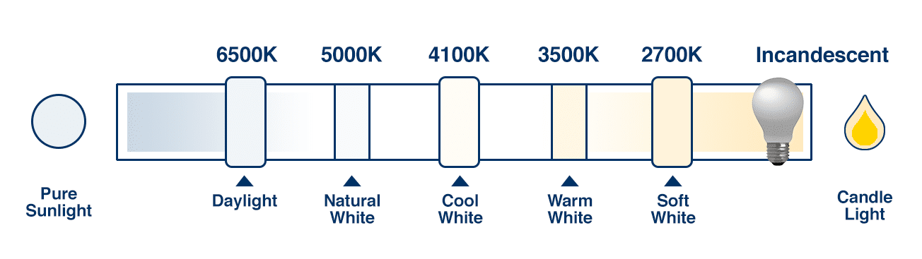
Have you noticed that some lights, such as traditional incandescent bulbs, emit a warm, yellowish light, while others emit a cooler, almost blue light? Don’t worry – your eyes aren’t playing tricks on you. Different bulbs emit light at different colour temperatures.

What is colour temperature? Let’s find out.

Colour temperature, also called “correlated colour temperature”, describes the appearance or tint of a particular light. Most bulbs emit a white light, but this white light can range from warm to cool. Think of colour temperature like you think of paint, where there are seemingly endless shades of white to choose from. In the same vein, there are a number of different colour temperatures for you to choose from when you’re selecting new light bulbs.

Some lamps, like incandescent bulbs, emit a warmer light, while other bulbs like LEDs provide a wider range of colour temperatures to choose from. Many people prefer the warmth of an incandescent bulb, but don’t realize that this type of light can be easily replicated by simply selecting the right energy-efficient bulb. If you’re considering upgrading to LEDs or other energy efficient bulbs, the light bulb colour temperature chart below can help you find the right colour temperature for your space. But before we start, let’s take a look at how to measure colour temperature.

How to Measure Colour Temperature

Correlated colour temperature is measured in degrees Kelvin on a scale from 1,000 to 10,000. Unlike measuring temperature in degrees celsius, the warmer a bulb’s light is, the lower its temperature will be. A cooler temperature will have a higher value.

For reference, candlelight has a colour temperature of about 2,000K, while sunlight has a temperature of about 6,000K.

colour temperature

Why Does Colour Temperature Matter?

Whether you’re looking for LEDs, CFLs, halogens, or incandescent bulbs, there are a vast variety of wattages and colour temperatures to choose from.

When we relied on incandescent bulbs for all of our lighting, we rarely had to consider colour temperature when replacing bulbs in our homes. Today’s energy efficient bulbs are available in a wide variety of colour temperatures, and many households who have begun switching to LEDs and CFLs experience dissatisfaction with their chosen bulb because it emits a different light than what they’re accustomed to. The light bulb colour temperature chart above can help you identify the correlated colour temperature of your current bulbs and find the perfect replacement for your space.

Choosing a bulb that provides an ideal colour temperature can have a significant impact on the feel and functionality of any space. If the colour temperature is too low (or too warm), you may not be able to see everything you need to see; for example, warm light isn’t always ideal for task lighting, but it is well-suited to ambient lighting. On the other hand, while cool temperatures are ideal for task lighting, a colour temperature that is too high (or too cool) may prevent you from achieving the calm or relaxed feeling you want out of your space.

When to Use Warm or Cool Light

No matter what space you’re lighting, it’s important to balance warm and cool temperatures. As a general rule, warmer temperatures are more calming, inviting, and relaxing, while cooler colour temperatures are often used to enhance concentration in places like schools or offices.

Warm White: 2,000-3,000K

Because of their warm, inviting glow, warm white bulbs are ideal for use in:

  • Bedrooms: Cool, blue light can disrupt our circadian rhythms and negatively affect the quality of our sleep.
  • Bathrooms: Warmer tones can be more flattering.
  • Dining rooms: Try using a dimmable bulb so you can adjust the lighting as appropriate.
  • Living rooms: Warm light is ideal for ambient lighting.
  • Decorative outdoor lighting
  • Restaurant or commercial ambient lighting

Rating: 5 out of 5.

How Does Kites Fly?

I want to make it as simple as possible, so that people who are not familiar with physics or aerodynamics can also understand it.

Free body diagram of a kite:

There are three principal forces acting on the kite; the weight, the tension in the line, and the aerodynamic force.
The weight W always acts from the centre of gravity toward the center of the earth. The aerodynamic force is usually broken into two components (shown in blue).
The lift L, which acts perpendicular to the wind, and the drag D, which acts in the direction of the wind.

The best answer I can give is to fly the kite your but i’ll try my best to explain.(Its awesome)

the kite has three parts
1)the body
2)bridle (kanni) to pivot the kite
3)and control line (manja) to control it

The kite is more like floating than flying in the air. Because there are multiple forces in opposite direction that help it to float.
1)Gravity
2)Thrust
3)Air drag
4)Lift

The initial phase of flying the kite is the most difficult one because you have to get it high up in the air where its more windier. The windier it is the better the lift because lift is generated because the of difference between the air pressure below and above the kite. So the windier the better. The control line is used to propel the kite in forward direction by giving it a jerk.
Once you’ve got it high up in the air then you just hold the tension and kite with be at a certain height otherwise it will go as high as it can.

What is Rectifier & Operation?

In electronics, Rectifier circuit is the most used circuit because almost every electronic appliance operates on DC (Direct Current) but the availability of the DC Sources are limited such as electrical outlets in our homes provide AC (Alternating current). The rectifier is the perfect candidate for this job in industries & Home to convert AC into DC. Even our cell phone chargers use rectifiers to convert the AC from our home outlets to DC. Different types of Rectifiers are used for specific applications.

VS-26MB60A Vishay | Vishay VS-26MB60A, Bridge Rectifier, 25A 600V, 4-Pin D  34 | 145-1748 | RS Malta Online

We mainly have two types of voltage types present that are widely used these days. They are alternating and direct voltage types. These voltage types can be converted from one type to another using special circuits designed for that particular conversion. These conversions happen everywhere.

Our main supply which we get from power grids are alternating in nature and the appliances we use in our homes generally require a small DC voltage. This process of converting alternating current into direct current is given the name rectification. Converting AC to DC is preceded by further process which can involve filtering, DC-DC conversion and so on. One of the most common part of an electronic power supply is a bridge rectifier.

Many electronic circuits require rectified DC power supply for powering various electronic basic components from available AC mains supply. The simple bridge rectifier is used in a variety of electronic AC based power devices.

Another way to look at the rectifier circuit is that, it can be said to convert currents instead of voltages. This makes more intuitive sense, because we are more accustomed to using current to define a component’s nature. Concisely, a rectifier take a current which has both negative and positive components and rectifies it such that only the positive component of the current remains.

Bridge rectifiers are widely used in power supplies that provide necessary DC voltage for the electronic component or devices. The most efficient switching devices whose characteristics are known fully are diodes. In theory any solid-state switch which can be controlled or cannot be controlled can be used instead of the diodes.

Usually, the types of Rectifiers are classified based on their output. In this article, we will discuss many types of Rectifiers such as:

  1. Single Phase Rectifiers
  2. Three Phase Rectifiers
  3. Controlled Rectifiers
  4. Uncontrolled Rectifiers
  5. Half Wave Rectifiers
  6. Full Wave Rectifiers
  7. Bridge Rectifiers
  8. Center-Tapped Rectifiers

What is Rectifier?

A Rectifier is an electrical device that is made of one or more than one diodes that converts the alternating current (AC) into direct current (DC). It is used for rectification where the process below shows that how it convert AC into DC..

What is Rectification?

Rectification is the process of conversion of the alternating current (which periodically changes direction) into direct current (flow in a single direction).

Types Of Rectifiers

There are mainly two types of rectifiers:

  1. Uncontrolled Rectifier
  2. Controlled Rectifier

Bridge rectifiers are of many types and the basis for the classification can be many, to name a few, type of supply, bridge circuit’s configurations, controlling capability etc. Bridge rectifiers can be broadly classified into single and three phase rectifiers based on the type of input they work on. Both of these types include these further classifications which can be made into both single and three phase rectifiers.

The further classification is based on the switching devices the rectifier uses and the types are uncontrolled, half controlled and full controlled rectifiers. Some of the types of rectifiers are discussed below.

Based on the type of rectification circuit does, the rectifiers are classified into two categories.

  1. Half wave rectifier
  2. Full wave rectifier

Half wave rectifier only converts half of the AC wave into DC signal whereas Full wave rectifier converts complete AC signal into DC.

Bridge rectifier is the most commonly used rectifier in electronics and this report will deal with the working and making of one. Simple bridge rectifier circuit is the most popular method for full wave rectification.

We will discuss both the controlled and uncontrolled (half waves and full waves bridge) rectifiers in details with circuit diagrams and operation as follows.

Uncontrolled Rectifier:

The type of rectifier whose output voltage cannot be controlled is called an uncontrolled rectifier.

A rectifier uses switches to work. The switches can be of various types, broadly, controllable switches and uncontrollable switches. A diode is unidirectional device that allows the current flow in only one direction. The working of a diode is not controlled as it will conduct as long as it is forward biased.

With a configuration of diodes in any given rectifier, the rectifier is not fully in the operator’s control, so these types of rectifiers are called uncontrolled rectifiers. It does not allow the power to vary depending on the load requirement. So this type of rectifier is commonly used in constant or fixed power supplies.

Uncontrolled rectifier uses only diodes and they give a fixed output voltage depending only on the AC input.

Types Of Uncontrolled Rectifier:

Uncontrolled Rectifiers are further divided into two types:

  1. Half Wave Rectifier
  2. Full Wave Rectifier
Half Wave Rectifier:

A Type of rectifier that converts only the half cycle of the alternating current (AC) into direct current (DC) is known as halfwave rectifier.

  1. 1 Positive Half Wave Rectifier:

A half wave rectifier that converts only the positive half cycle and blocks the negative half cycle.

Positive & Negative Half Wave Rectifier
  1. 2 Negative Half Wave Rectifier:

A negative half wave rectifier converts only the negative half cycle of the AC into DC.

In all types of rectifiers, a half-wave rectifier is the simplest of them all as it is composed of only a single diode.

A diode allows the current flow in only one direction known as forward bias. A load resistor RL is connected in series with the diode.

Positive Half Cycle:

During the positive half cycle, the diode terminal anode will become positive and the cathode will become negative known as forward bias. And it will allow the positive cycle to flow through.

Negative Half Cycle:

During the negative half cycle, the anode will become negative and the cathode will become positive, which is known as reverse bias. So the diode will block the negative cycle.

So when an AC source is connected to the half-wave rectifier, only half cycle will flow through it as shown in the figure below.

The output of this rectifier is taken across the load resistor RL. if we look at the input-to-output graph, it shows a pulsating positive half cycle of the input.

The output of the half wave rectifier has too many ripples & it is not very practical to use this output as DC source. To smooth this pulsating output, a capacitor is introduced across the resistor. The capacitor will charge during the positive cycle and discharge during the negative cycle to give out a smooth output signal.

Such types of rectifiers waste the power of AC input’s half cycle. 

2.Full Wave Rectifier:

A full wave rectifier converts both positive and negative half cycles of the AC (alternating current) into DC (direct current). It provides double output voltage compared to the halfwave rectifier

A full wave rectifier is made up of more than one diode.

There are two types of full wave rectifier.

  1. Bridge Rectifier
  2. Center-Tap Rectifier
2.1 Bridge Rectifier

A bridge rectifier uses four diodes to convert both half cycle of the input AC  into DC output.

In this type of rectifier, the diodes are connected in a specific form as given below.

Positive Half Cycle:

During input positive half cycle, the diode D1 & D2 becomes forward bias while D3 & D4 becomes reverse bias. The diode D1 & D2 form a closed loop that provides a positive output voltage across the load resistor RL.

Negative Half Cycle:

During the negative half cycle, the diode D3 & D4 becomes forward bias while D1 & D2 becomes reverse bias. But the polarity across the load resistor RL remains the same and provides a positive output across the load.

The output of full wave rectifier has low ripples compared to half-wave rectifier but still, it’s not smooth and steady.

In order to make the output voltage smooth & steady, a capacitor is placed at the output as shown in the figure below.

Working of Bridge Rectifier Circuit

From the circuit diagram it is apparent that the diodes are connected in a particular fashion. This unique arrangement gives the converter its name. In bridge rectifier, voltage that is given as the input can be from any source. It can be from a transformer that is used to step up or down the voltage or it can be from the mains of our domestic power supply.  In this article, we are using a 6-0-6 centre tapped transformer for providing AC voltage.

In the first phase of working of the rectifier, during the positive half cycle, diodes D3-D2 get forward biased and conducts. Diodes D1-D4 gets reversed biased and do not conduct in this half cycle, acting as open switches. Thus, we get a positive half cycle at the output. Conversely, in the negative half cycle, diodes D1-D4 get forward biased, and start conducting whereas diodes D3-D2 gets reversed biased and do not conduct in this half cycle.

Again, we get a positive half cycle at the output. At the end of the rectification process, the negative part of the AC current is converted into a positive cycle. The output from the rectifier is two half-positive pulses with the same frequency and magnitude as that of the input.

In contrast to the working of a half-wave rectifier, the full bridge rectifier has another branch which allows it to conduct for the negative half of the voltage waveform which the half-bridge rectifier had no means of doing. So the average voltage at the output of the full bridge rectifier is double than that of the half-bridge rectifier.

Although we use four individual power diodes to make a full wave bridge rectifier, pre-made bridge rectifier components are available “off-the-shelf” in a range of different voltage and current sizes that can be used directly to make a working circuit.

he output voltage waveform after the rectification is not a proper DC, so we can try to make it more into a DC waveform using a capacitor for filtering purpose. Smoothing or reservoir capacitors that are connected in parallel with the load across the output of the full wave bridge rectifier circuit increases the average DC output level to the required average DC voltage at the output because the capacitor not only acts as a filtering component, but it also periodically charges and discharges effectively increasing the output voltage.

Capacitor charge till the waveform goes to its peak and discharges uniformly into the load circuit when waveform starts going low. So when the output is going low, capacitor maintains the proper voltage supply into the load circuit, hence creating the DC.

Advantages of a Bridge Rectifier:

  1. Low ripples in the output DC signal
  2. High rectifier efficiency
  3. Low power loss

Disadvantages of Bridge Rectifier:

  1. Bridge rectifier is more complex than a half-wave rectifier
  2. More power loss compared to centre tapped full wave rectifier.
Center-Tap Rectifier

This type of full-wave rectifier uses a center-tap transformer & two diodes.

A center-tap transformer is a dual-voltage transformer that has two inputs (I1 & I2) and three output terminals (T1, T2, T3). The T2 terminal is connected to the center of the output coil which acts as a reference ground (o volt reference). The T1 terminal produces positive voltage and the T3 terminal produces negative voltage with respect to the T2.

The design of the center-tap rectifier is given below:

Postive Half Cycle:

During the input positive half cycle, the T1 will produce positive and T2 will produce a negative voltage. The diode D1 will become forward bias & diode D2 will become reverse bias. This makes a close path from T1 to T2 through the load resistor RL as shown below.

Negative Half Cycle:

Now during the input negative half cycle, T1 will generate negative cycle & T2 will generate a positive cycle. This will put the diode D1 into reverse bias & diode D2 in forward bias. But the polarity across the load resistor RL is still the same as the current takes the path from T3 to T1 as shown in the figure below.

The DC output of a center-tap rectifier also has ripples and it’s not smooth & steady DC. A capacitor at the output will remove the ripple and make a steady DC output.

Controlled Rectifier:

A type of rectifier whose output voltage can be varied or changed is called controlled rectifier.

The need for a controlled rectifier is apparent when we look into the shortcomings of an uncontrolled bridge rectifier. To make an uncontrolled rectifier into a controlled one we use current-controlled solid-state devices such as SCRs, MOSFETs, and IGBTs. We have the full control when SCRs are switched ON or OFF based on the gate pulses we apply to it. These are generally more preferred than their uncontrolled counterparts.

It is composed of one or more than one SCR (Silicon Controlled Rectifier).

An SCR, also known as thyristoris a three-terminal diode. These terminals are Anode, Cathode & a control input known as Gate.

Just like a simple diode an SCR conduct in forward bias and blocks current in reverse bias but it only starts forward conduction when there is a pulse at the gate input. So the output voltage can be controlled using the gate input.

Types of controlled rectifier

There are two types of controlled rectifier.

Half Wave Controlled Rectifier

The half wave controlled rectifier is made up of a single SCR (Silicon Controlled Rectifier).

Half wave controlled rectifier has the same design as the half wave uncontrolled rectifier except we replace the diode with an SCR as shown in figure down below.

An SCR does not conduct in reverse bias, so it will block the negative half cycle.

During the positive half cycle, the SCR will conduct current on one condition when a pulse is applied to the gate input. The gate input is, of course, a periodic pulse signal which is designed to activate the SCR at each positive half cycle.

In this way, we can control the output voltage of this rectifier.

The output of the SCR is also a pulsating DC voltage/current. These pulses are removed by using a capacitor parallel to the load resistor RL.

Full Wave Controlled Rectifier

A type of rectifier that converts both positive and negative half cycle of the AC into DC as well as controls the output amplitude is known as a full wave controlled rectifier.

Just like uncontrolled rectifier, controlled full wave rectifier has two types.

Controlled Bridge Rectifier

In this rectifier, the diode bridge is replaced by an SCR (Thyristor) bridge with the same configuration as shown in the figure below.

Positive Half Cycle:

During the positive cycle, the SCR (thyristor) T1 & T2 will conduct when the gate pulse is applied. T3 & T4 will be reversed bias, so they will block the current. The output voltage will be established across the load resistor RL as shown below.

Negative Half Cycle:

During the negative half cycle, the thyristor T3 & T4 will become forward bias considering the gate input pulse & the T1 & T2 will become reverse bias. The output voltage will appear across the load resistor RL.

At the end of the output, a capacitor is used to remove the ripples and makes the output steady & smooth.

Single Phase and Three Phase Rectifiers

This classification is based on the type of input a rectifier works on. The naming is pretty straightforward. When the input is single phase, the rectifier is called a single phase rectifier and when the input is three phase, it is called a three phase rectifier.

The single phase bridge rectifier consists of four diodes, whereas a three phase rectifier uses six diodes arranged in a particular fashion to get the desired output. These can be controlled or uncontrolled rectifiers depending on the switching components used in each rectifier such as diodes, Thyristors, and so on.

Comparison Of Rectifiers

The following table shows the compassion between different types of rectifiers such as half wave rectifier, full wave rectifier and center tapped rectifier.

Applications Of Rectifiers

Basically, almost all electronic circuits operated on DC voltages. The main purpose of using rectifier is for rectification which means converting AC voltages to DC Voltages. Its mean, rectifiers are used in almost all power rectification and electronics appliances.

Below is the list of common applications and uses of different Rectifiers.

  1. Rectification i.e. converting DC Voltages to AC Voltages.
  2. Rectifiers are used in electric welding to provide the polarized voltage.
  3. It is also used in traction, rolling stock and three phase traction motors used for running trains.
  4. Half wave rectifiers are used in mosquito repellent and soldering iron.
  5. Half wave rectifier also used in AM Radio as a detector and signal peak detector.
  6. Rectifiers also used in modulation, demodulation and voltage multipliers.

Rating: 5 out of 5.

Switch Mode Power Supply

Power supply circuit plays an essential role in every electrical and electronic circuit to provide the electrical power to the owl circuit or loads like machines, computers, etc. These different loads require different forms of power at various ranges and characteristics. So, the power is converted into the desired form by using different power converters. Basically, different loads work with various types of power supplies like SMPS (switch mode power supply), AC power supply, AC to DC power supply, programmable power supply, high voltage power supply & uninterruptible power supply.

Switch Mode Power Supply

What is SMPS (Switch-Mode Power Supply)?

SMPS is defined as, when the power supply is included with the switching regulator from converting electrical power from one form to another form with necessary characteristics is called switch mode power supply. This power supply is used to attain regulated DC o/p voltage from the DC i/p voltage or unregulated AC.

SMPS

Typologies of SMPS

Typologies of SMPS are categorized into different types such as AC-DC converter, DC-DC converter, Forward Converter and Flyback converter.

Working principle of Switch Mode Power Supply

The working of a switch mode power supply typologies is discussed below.

DC-DC Converter SMPS Working

In this power source, a high voltage DC power is directly acquired from a DC power source. Then, this high voltage DC power is switched usually in the range of 15KHz-5KHz. And, then it is fed to a step down transformer unit of 50Hz. The o/p of this transformer is fed to the rectifier, them this rectified o/p power is used as a source for loads, and the oscillator ON time is controlled and a closed loop regulator is formed.

DC to DC converter SMPS

The switching-power supply o/p is regulated by using Pulse Width Modulation shown in the above circuit, the switch is driven by the PWM oscillator, then indirectly the step down transformer is controlled when the power fed to the transformer. Therefore, the o/p is controlled by the pulse width modulation, as this o/p voltage and PWM signal are inversely proportional to each other. If the duty cycle is 50%, then the max power is transferred through the transformer, and if the duty cycle drops, then the power in the transformer also drops by decreasing the power dissipation.

C -DC Converter SMPS Working

This type of SMPS has an AC i/p and it is converted into DC by using rectifier & filter. This unregulated DC voltage is fed to the power factor correction circuits as it is affected. This is because around the voltage peaks, the rectifier draws short current pulses having significantly high-frequency energy that affects the power factor to reduce.

AC to DC converter SMPS

Know All About Switch Mode Power Supply

Power supply circuit plays an essential role in every electrical and electronic circuit to provide the electrical power to the owl circuit or loads like machines, computers, etc. These different loads require different forms of power at various ranges and characteristics. So, the power is converted into the desired form by using different power converters. Basically, different loads work with various types of power supplies like SMPS (switch mode power supply), AC power supply, AC to DC power supply, programmable power supply, high voltage power supply & uninteruptable power supply.

Switch Mode Power Supply

What is SMPS (Switch-Mode Power Supply)?

SMPS is defined as, when the power supply is included with the switching regulator from converting electrical power from one form to another form with necessary characteristics is called switch mode power supply. This power supply is used to attain regulated DC o/p voltage from the DC i/p voltage or unregulated AC.

SMPS
SMPS

SMPS is a complicated circuit like other power supplies, it supplies from a source to the loads. MPS is crucial for different electrical and electronic appliances which consumes power and also for designing electronic projects.

Typologies of SMPS

Typologies of SMPS are categorized into different types such as AC-DC converter, DC-DC converter, Forward Converter and Fly back converter.

Working principle of Switch Mode Power Supply

The working of a switch mode power supply typologies is discussed below.

DC-DC Converter SMPS Working

In this power source, a high voltage DC power is directly acquired from a DC power source. Then, this high voltage DC power is switched usually in the range of 15KHz-5KHz. And, then it is fed to a step down transformer unit of 50Hz. The o/p of this transformer is fed to the rectifier, them this rectified o/p power is used as a source for loads, and the oscillator ON time is controlled and a closed loop regulator is formed.

DC to DC converter SMPS

The switching-power supply o/p is regulated by using Pulse Width Modulation shown in the above circuit, the switch is driven by the PWM oscillator, then indirectly the step down transformer is controlled when the power fed to the transformer. Therefore, the o/p is controlled by the pulse width modulation, as this o/p voltage and PWM signal are inversely proportional to each other. If the duty cycle is 50%, then the max power is transferred through the transformer, and if the duty cycle drops, then the power in the transformer also drops by decreasing the power dissipation.

AC -DC Converter SMPS Working

AC to DC converter SMPS

It is almost related to the above discussed converter, but in the place of DC power supply, here we have used AC i/p. So, the mixture of the rectifier &filter, this block diagram is used for converting the AC to DC and the switching operation is done by using a power MOSFET amplifier. The MOSFET transistor consumes low on-resistance & can resist high currents. The frequency of the switching is selected such that it must be kept low to normal human beings (above 20KHz) and action of switching is controlled by a feedback using the PWM oscillator.

Again, this AC voltage is fed to the o/p of the transformer shown in the above figure to step up or step down the levels of voltage. Then, the this transformer’s o/p is rectified & smoothed by using the o/p filter and a rectifier. The o/p voltage is controlled by a feedback circuit by likening it with the reference voltage.

Fly-back Converter SMPS Working

The SMPS circuit which has very low o/p power (less than 100W) is called as fly-back converter SMPS. This type of SMPS is very low and simple circuit compared with other SMPS circuits. This type of SMPS is used for low power applications.

Fly-back Converter type SMPS

The unregulated i/p voltage with a constant magnitude is changed into a preferred o/p voltage by switching fast using a MOSFET; the frequency of switching is around 100 kHz. The voltage isolation can be attained by using a transformer. The operation of the switch can be controlled by using a PWM while executing a practical fly-back converter.

Fly-back transformer shows dissimilar characteristics compared to normal transformer.Fly-back transformer includes two windings which acts as a magnetic coupled inductor. The o/p of this transformer is delivered through a capacitor and diode for filtering as well as rectification. As shown in the above figure, the o/p of the SMPS can be taken as voltage across the filter capacitor.

Forward Converter type SMPS Working

This type of SMPS is almost same to the fly back converter type SMPS. But, in this type of SMPS a control is connected at the o/p of the secondary winding of the transformer to control the switch. As compared to the fly back converter, the filtering and rectification circuit is complicated.

Forward Converter type SMPS

This is also called as a DC-DC buck converter, along with a transformer which is used for scaling and isolation. In addition to the “D1” diode & “C” capacitor, an inductor L & a diode D are connected at the end of the o/p. If ‘S’ switch gets switched ON, then the i/p is given to the transformer’s primary winding. Therefore, a scaled voltage is produced at the transformer’s secondary winding.

Therefore, the D1 diode gets forward biased & scaled voltage is passed through the LPF proceeding the load. When the switch S is turned ON, then the currents through the winding reaches to zero, However the current through the inductive filter & load cannot be changed shortly, and a lane is offered to this current by the coasting diode D2. By using the filter inductor, the required voltage across the D2 diode & to keep the electromagnetic force necessary for maintaining the stability of the current at inductive filter. Even though the current is falling against the o/p voltage, almost the constant o/p voltage is sustained with the existence of the large capacitive filter. It is regularly used for various switching applications with a 100 W to 200 W power range.

This is all about switch mode power supply and its types which involves Buck converter, Buck-boost converter Self Oscillating fly-back converter, Boost converter, Cuk, Sepic, Boost-buck. But, a few types of SMPS’s are discussed in this article they are AC-DC converter, DC-DC converter, Forward and Fly-back converter. Furthermore, any information regarding the types of SMPS, fell free to give your feedback to give your suggestions, comments in the comment section below.

Rating: 5 out of 5.

भौतिक एवं रासायनिक परिवर्तन MCQs

प्रश्न 1. निम्नलिखित प्रक्रमों के अंतर्गत होने वाले परिवर्तनों को भौतिक अथवा रासायनिक परिवर्तन के रूप में वर्गीकृत कीजिए

(क) प्रकाश संश्लेषण
(ख) जल में शक्कर को घोलना
(ग) कोयले को जलाना
(घ) मोम को पिघलाना
(च) ऐलुमिनियम के टुकड़े को पीटकर उसका पतला. पत्र (फॉइल) बनाना।
(छ) भोजन का पाचन

उत्तर. (क) प्रकाश संश्लेषण – रासायनिक परिवर्तन
(ख) जल में शक्कर को घोलना – भौतिक परिवर्तन
(ग) कोयले को जलाना – रासायनिक परिवर्तन
(घ) मोम को पिघलाना – भौतिक परिवर्तन
(च) ऐलुमिनियम के टुकड़े को पीटकर
उसका पतला पत्र (फॉइल) बनाना – भौतिक परिवर्तन
(छ) भोजन का पाचन – रासायनिक परिवर्तनप्रश्न

प्रश्न 2.बताइए कि निम्नलिखित कथन सत्य हैं अथवा असत्य। यदि कथन असत्य हो तो, अपनी अभ्यास पुस्तिका में उसे सही करके लिखिए।

(क) लकड़ी के लट्टे को टुकड़ों में काटना एक रासायनिक परिवर्तन है। (सत्य/असत्य)
(ख) पत्तियों से खाद का बनना एक भौतिक परिवर्तन है। (सत्य/असत्य)
(ग) जस्ते (जिंक) लेपित लोहे के पाइपों में आसानी से जंग नहीं लगती है। (सत्य/असत्य)
(घ) लोहा और जंग एक ही पदार्थ हैं। (सत्य/असत्य)
(च) भाप का संघनन रासायनिक परिवर्तन नहीं है। (सत्य/असत्य)

उत्तर. (क) असत्य; लकड़ी के लट्टे को टुकड़ों में काटना एक भौतिक परिवर्तन है।
(ख) असत्य; पत्तियों से खाद का बनना एक रासायनिक परिवर्तन है।
(ग) सत्य
(घ) असत्य; लोहा और जंग अलग-अलग पदार्थ हैं।
(च) सत्य

प्रश्न 3. निम्नलिखित कथनों में रिक्त स्थानों को भरिए

(क) जब कार्बन डाइऑक्साइड को चूने के पानी में प्रवाहित किया जाता है, तो यह … …….. के बनने
के कारण दूधिया हो जाता है।
(ख) खाने के सोडे का रासायनिक नाम …………….. है।
(ग) ऐसी दो विधियाँ, जिनके द्वारा लोहे को जंग लगने से बचाया जा सकता है … ………. और ………. हैं।
(घ) ऐसे परिवर्तन भौतिक परिवर्तन कहलाते हैं, जिनमें किसी पदार्थ के केवल …………… गुणों में परिवर्तन
होता है।
(च) ऐसे परिवर्तन जिनमें नए पदार्थ बनते हैं, ……………. परिवर्तन कहलाते हैं।

उत्तर. (क) कैल्सियम कार्बोनेट
(ख) सोडियम हाइड्रोजन कार्बोनेट
(ग) यशद्-लेपन; विद्युत लेपन
(घ) भौतिक
(च) रासायनिक

प्रश्न 4. जब नींबू के रस में खाने का सोडा मिलाया जाता है, तो बुलबुले बनते हैं और गैस निकलती है। यह किस प्रकार का परिवर्तन है? समझाइए।

उत्तर. जब नींबू के रस में खाने का सोडा मिलाया जाता है तो बुलबुले बनते हैं और गैस निकलती है। यह एक रासायनिक परिवर्तन है क्योंकि इसमें एक नए पदार्थ की उत्पत्ति होती है तथा कार्बन डाइऑक्साइड गैस बाहर निकलती है। .

प्रश्न 5. जब कोई मोमबत्ती जलती है, तो भौतिक और रासायनिक परिवर्तन दोनों होते हैं। इन परिवर्तनों की पहचान कीजिए। ऐसे ही किसी ज्ञात प्रक्रम का एक और उदाहरण दीजिए, जिसमें भौतिक और रासायनिक परिवर्तन दोनों होते हैं।

उत्तर. मोमबत्ती के जलने में सबसे पहले मोमबत्ती का मोम पिघलता है फिर वाष्प बनकर जलता है। इस प्रक्रम में मोम का पिघलना एक भौतिक परिवर्तन है क्योंकि मोम को दुबारा ठोस अवस्था में लाया जा सकता है तथा इसमें कोई नया पदार्थ नहीं बनता है जब मोम के वाष्प जलते हैं तो धुआँ और कार्बन डाइऑक्साइड गैस उत्पन्न होते हैं जो कि नए पदार्थ हैं। अतः यह प्रक्रम रासायनिक परिवर्तन है।शुष्क सैलों वाली टॉर्च में बल्ब का जलना एक अन्य उदाहरण है जिसमें भौतिक और रासायनिक दोनों प्रकार के परिवर्तन होते हैं क्योंकि बल्ब का जलना व बुझना एक भौतिक परिवर्तन है, इसमें किसी नए पदार्थ की उत्पत्ति नहीं होती है।शुष्क सैल से विद्युत की उत्पत्ति उसमें उपस्थित रासायनिक पदार्थ से प्राप्त होती है जो कि एक रासायनिक परिवर्तन है।

प्रश्न 6. आप यह कैसे दिखाएँगे कि दही का जमना एक रासायनिक परिवर्तन है?

उत्तर. जब दूध में कुछ खट्टा पदार्थ डालकर उसे कुछ घंटों के लिए रख दिया जाता है तो हमें दही प्राप्त होती है। परंतु दही को किसी भी तरीके से दुबारा दूध में परिवर्तित नहीं किया जा सकता। क्योंकि दही दूध से भिन्न पदार्थ है इसलिए दही का जमना एक रासायनिक परिवर्तन है।

प्रश्न 7. समझाइए कि लकड़ी के जलने और उसे छोटे टुकड़ों में काटने को दो भिन्न प्रकार के परिवर्तन क्यों माना जाता है?

उत्तर. लकड़ी के जलने से धुआँ तथा राख बनते हैं अर्थात् लकड़ी के गुण बदल जाते हैं तथा नए पदार्थों की उत्पत्ति होती है इंसलिए लकड़ी का जलना एक रासायनिक परिवर्तन है।

परन्तु जब लकड़ी के लट्टे को छोटे-छोटे टुकड़ों में काटा जाता है तो लकड़ी के गुणों में कोई परिवर्तन नहीं होता और न ही कोई नया पदार्थ बनता है। इसलिए लकड़ी के लट्टे को छोटे-छोटे टुकड़ों में काटना एक भौतिक परिवर्तन है। अतः लकड़ी का जलना और उसे छोटे टुकड़ों में काटना दो भिन्न कॉपर सल्फेट परिवर्तन हैं।

प्रश्न 8. कॉपर सल्फेट के क्रिस्टल कैसे बनाते हैं, इसका वर्णन कीजिए।

उत्तर. किसी बीकर में एक कप जल लेकर उसमें तनु सल्फ्यूरिक अम्ल की कुछ बूंदें मिलाइए। जल को गर्म कीजिए। जब जल उबलना आरंभ कर दे, तो इसमें धीरे-धीरे कॉपर सल्फेट का चूर्ण निरंतर चलाते हुए मिलाएँ (जैसा कि चित्र में दर्शाया है)। कॉपर सल्फेट का चूर्ण मिलाना तब तक जारी रखें, जब तक कि उसमें और कॉपर सल्फेट घुलना बंद हो जाए। विलयन को

फिल्टर पेपर की सहायता से छान लीजिए। इसे ठंडा होने दीजिए। ज़ब विलयन ठंडा हो रहा हो, तो उसे हिलाना नहीं चाहिए। आप देखेंगे कि ठंडा होने पर बीकर के तल पर कॉपर सल्फेट के क्रिस्टल प्राप्त हो जाएँगे।

प्रश्न 9. समझाइए कि लोहे के गेट को पेंट करने से उसका जंग लगने से बचाव किस कारण से होता है?

उत्तर. हम जानते हैं कि लोहे को जंग लगने के लिए वायु तथा नमी दोनों की आवश्यकता होती है। जब लोहे के गेट को पेंट किया जाता है तो लोहे का संपर्क वायु व नमी से टूट जाता है जिस कारण लोहे का गेट जंग से बच जाता है।

प्रश्न 10. समझाइए कि रेगिस्तानी क्षेत्रों की अपेक्षा समुद्र-तटीय क्षेत्रों में लोहे की वस्तुओं में जंग अधिक क्यों, लगती है?

उत्तर. समुद्र-तटीय क्षेत्रों में समुद्र के कारण वायु में नमी की मात्रा अधिक होती है जिस कारण लोहे की वस्तुओं को अधिक जंग लगता है जबकि रेगिस्तानी क्षेत्रों में वायु में नमी की मात्रा न के बराबर होती है जिस कारण लोहे की वस्तुओं को कम जंग लगता है। अतः रेगिस्तानी क्षेत्रों की अपेक्षा समुद्र-तटीय क्षेत्रों में लोहे की वस्तुओं में अधिक जंग लगता है।

प्रश्न 11. हम रसोई में जिस गैस का उपयोग करते हैं, वह द्रवित पेट्रोलियम गैस (LPG) कहलाती है। सिलिंडर में LPG द्रव के रूप में होती है। सिलिंडर से बाहर आते ही यह गैस में परिवर्तित हो जाती है (परिवर्तन A); फिर यही गैस जलती है (परिवर्तन B)। निम्नलिखित कथन इन परिवर्तनों से संबंधित हैं। सही कथन का चयन कीजिए।

(क) प्रक्रम A एक रासायनिक परिवर्तन है।
(ख) प्रक्रम B एक रासायनिक परिवर्तन है।
(ग) प्रक्रम-A और प्रक्रम-B दोनों ही रासायनिक परिवर्तन हैं।
(घ) इनमें से कोई भी प्रक्रम रासायनिक परिवर्तन नहीं है।

उत्तर. (ख) प्रक्रम-B एक रासायनिक परिवर्तन है।

प्रश्न 12. अवायवीय जीवाणु जैविक अपशिष्ट पदार्थों को अपघटित कर जैव गैस (बायोगैस) बनाते हैं (परिवर्तन-A)। फिर जैव गैस ईंधन के रूप में जलाई जाती है (परिवर्तन-B)। निम्नलिखित कथन इन परिवर्तनों से संबंधित हैं। सही कथन चुनिए।

(क) प्रक्रम-A एक रासायनिक परिवर्तन है।
(ख) प्रक्रम-B एक रासायनिक परिवर्तन है।
(ग) प्रक्रम-A और प्रक्रम-B दोनों ही रासायनिक परिवर्तन हैं।
(घ) इनमें से कोई भी प्रक्रम रासायनिक परिवर्तन नहीं है।

उत्तर. (ग) प्रक्रम-A और प्रक्रम-B दोनों ही रासायनिक परिवर्तन हैं।

Some Common Applications of Logic Gates

During the course of discussion about various digital logic gates, we have mainly discussed about the design, property and operation of them. In this article we will look at various applications of logic gates. Their applications are determined mainly based upon their truth table i.e. their mode of operations. In the following discussion we will look at the applications of basic logic gates as well as many other normal logic gates as well.

Application of OR gate

Wherever the occurrence of any one or more than one event is needed to be detected or some actions are to be taken after their occurrence, in all those cases OR gates can be used. It can be explained with an example.

Suppose in an industrial plant if one or more than one parameter exceeds the safe value, some protective measure is needed to be done. In that case OR gate is used. We are going to show this with the help of a diagram.
application of or gate
The above figure is a typical schematic diagram where an OR gate is used to detect exceed of temperature or pressure and produce command signal for the system to take required actions.

Application of AND Gate

There are mainly two applications of AND gate as Enable gate and Inhibit gate. Enable gate means allowance of data through a channel and Inhibit gate is just the reverse of that process i.e. disallowance of data through a channel. We are going to show an enabling operation to understand it in an easier way. Suppose in the measurement of frequency of a pulsed waveform. For measurement of frequency a gating pulse of known frequency is sent to enable the passage of the waveform whose frequency is to be measured. The diagram below shows the arrangement of the above explained operation.
application of and gate

Application of Ex-OR/Ex-NOR Gate

These type of logic gates are used in generation of parity generation and checking units. The two diagrams below shows the even and odd parity generator circuits respectively for a four data.
parity generation using ex

With the help of these gates parity check operation can be also performed. The diagrams below show even and odd parity check.
parity checker
Figure (a) shows the parity check using Ex-OR gates and the figure (b) shows the parity check using Ex-NOR gates.

Application of NOT gate or Inverters

NOT gates are also known as inverter because they invert the output given to them and show the reverse result. Now the CMOS inverters are commonly used to build square wave oscillators which are used for generating clock signals. The advantage of using these is they consume low power and their interfacing is very easy compared to other logic gates.
square wave oscillator
The above figure shows the most fundamental circuit made of ring configuration to generate square wave oscillator. The frequency of this type generator is given by

Where, n represents the number of inverters and tp shows the propagation delay per gate.

Rating: 5 out of 5.

X OR Gate & X NOR Gate

What is a XOR Gate?

An XOR gate (also known as an EOR, or EXOR gate) – pronounced as Exclusive OR gate – is a digital logic gate that gives a true (i.e. a HIGH or 1) output when the number of true inputs is odd. An XOR gate implements an exclusive or, i.e. a true output result occurs if one – and only one – of the inputs to the gate is true. If both inputs are false (i.e. LOW or 0) or both are true, a false output results.

XOR represents the inequality function, i.e., the output is true if the inputs are not alike otherwise the output is false. A common way to remember the XOR is “must have one or the other, but not both”.

Another way to look at an XOR gate: a modulo sum of two variables in a binary system looks like this:
equation
The logic gate performs this modulo sum operation without including carry is known as XOR gate. An XOR gate is normally two inputs logic gate where, output is only logical 1 when only one input is logical 1. When both inputs are equal, that is either both are 1 or both are 0, the output will be logical 0.

This is the reason an XOR gate also called anti-coincidence gate or inequality detector. This gate is called as XOR or exclusive OR gate because, its output is only 1 when one of its input is exclusively 1.

XOR Gate Truth Table

equation

The truth table of an XOR gate is given below:

The binary operation of above truth table is known as exclusive OR operation and it is represented as, A ⊕ B. The symbol of exclusive OR operation is represented by a plus ring surrounded by a circle ⊕.

Realization of Two Inputs XOR Gate

The above expression, A ⊕ B can be simplified as,
equation

Let us prove the above expression.
In first case consider, A = 0 and B = 0.

In second case consider, A = 0 and B = 1.

In third case consider, A = 1 and B = 0.

In fourth case consider, A = 1 and B = 1.

So it is proved that, the Boolean expression for A ⊕ B is AB ̅ + ĀB, as this Boolean expression satisfied all output states respect to inputs conditions, of an XOR gate.
From this Boolean expression one can easily realize the logical circuit of an XOR gate and this will be as show,
x or gate logic circuit

Logical Symbol of XOR Gate

logical symbol of xor gate

An XOR gate is logically represented as,
https://www.youtube.com/embed/rOue27ugig0

More than Two Inputs XOR Gate

As we told already, that XOR gates are two inputs gate, but XOR operation of more than two inputs then can be realized by using more than one or two inputs XOR gate. More than two inputs XOR operation is that, when odd number of inputs in the gate are 1, the output is 1 and when none or even number of inputs are 1, the output is logical 0.

3 input XOR Gate

Let us realize an XOR gate with three inputs A, B, and C.

xor truth table
truth table
three input x or gate

Now, as per definition of XOR operation with more than three inputs, the truth table would be,

This truth table can be elaborated as,

From the above elaborated truth table it is found that, XOR operation of three binary variables is equivalent to, XOR operation one variable with result of XOR operations of other two variables.
From above truth table,
truth table

What is a XNOR Gate?

The XNOR gate (also known as a XORN’T, ENOR, EXNOR or NXOR) – and pronounced as Exclusive NOR – is a digital logic gate whose function is the logical complement of the exclusive OR (XOR) gate. Logically, an XNOR gate is a NOT gate followed by a XOR gate.

As we know that XOR operation of inputs A and B is A ⊕ B, therefore XNOR operation those inputs will be (A + B) ̅. That means, output of XOR gate is inverted in XNOR gate. In XOR operation, the output is only 1 when only one input is 1.

The output is logical 0 when both inputs are same that means they are either 1 or 0. But in the case of XNOR gate, the output is 0 when only one input is 0 and the output is 1 when both inputs are same that is either both of them are 0 or 1.

XNOR Gate Truth Table

truth table xnor gate

The truth table of the XNOR gate is shown below:

The logical XNOR operation is represented by ⊙. That is a dot surrounded by circle. The expression of XNOR operation between variable A and B is represented as A ⊙ B.
Now again, the truth table is satisfied by the equation AB + ĀB ̅.

Hence, it is proved that A ⊙ B = AB + ĀB ̅. The same can be proved by using K-map also.

Realization of XNOR Gate

logic circuit of x nor gate
symbol of xnor gate

The expression of XNOR operation can be realized by using two NOT gates, two AND gates and one OR gate as followers,

The symbol of XNOR gate.
https://www.youtube.com/embed/BqtLFTJThaQ

3 Input XNOR Gate

Like XOR gate, an XNOR gate only exists with two inputs but for XNOR operation with more than two inputs, we have to use more than one XNOR gates.

three input x nor gate

XNOR operation with more than two inputs is like that, when there are odd numbers of inputs are in high or logical 1 condition, the output will be 0 in otherwise the output will be 1.

Now,

From this elaborate truth table, the logical symbol of three inputs XNOR gate can be represented as,

Applications of XOR Gates

The main application of the Exclusive OR gate is in the operation of half and full adder. If we look at the truth table carefully we will find that the first three results are totally satisfying the process of binary addition but in the last input sequence i.e. when both the inputs are 1 the result according to the rule of addition should be 0 with a carry 1. In the truth table we are getting the desired 0 but a missing 1.

circuit diagram of half adder

To solve this problem during designing the circuit of an adder an AND gate is added to the Ex-OR gate in parallel. We will show the circuit of the adder in detail.

From the above diagram, we can see that in the circuit of a half adder the two inputs are going through an Exclusive-OR gate and through an AND gate parallelly. And with this circuit’s operation we get the total process of binary addition smoothly.

Rating: 5 out of 5.

NOT Gate

What is a NOT Gate?

NOT gate is a logic gate that inverts the digital input signal. For this reason, a NOT gate is sometimes is referred to as an inverter (not to be confused with a power inverter). A NOT gate always has high (logical 1) output when its input is low (logical 0). Conversely, a logical NOT gate always has low (logical 0) output when the input is high (logical 1). The logical symbol for a NOT gate is shown below:
not gate symbol

If the input binary variable of a NOT gate is considered as A, then the output binary variable of the gate will be Ā. As the symbol of not operation is ( – ) bar. If the value of A is 1.
then Ā = 0 and in the opposite if the value of A is then Ā = 1.

Truth tables list the output of a particular digital logic circuit for all the possible combinations of its inputs. The truth table of a NOT gate can be represented as,
not gate truth table

NOT Gate Transistor Circuit Diagram

A NOT gate can easily be realized by using a simple bipolar transistor. The transistor circuit diagram of a NOT gate (also known as a transistor inverter) is shown below:
NOT Gate Transistor Circuit Diagram

The transistor diagram above will be used to demonstrate how a NOTE gate works.

How a NOT Gate Works

Let us examine the above transistor circuit when a high input voltage is applied, i.e. +5V.
how does a not gate work
In this condition, the transistor T gets enough base potential to make it ‘ON’.

As soon as the transistor becomes ON, the supply voltage (+5V) at B will get a path to the earth through the resistor R. At ON condition the transistor will behave short-circuited ideally, hence entire supply voltage will drop across resistor R and no voltage will appear at X and hence the output of the inverter or NOT gate will be zero. In actual fact, there will be some voltage drop across the collector and emitter even at ON condition, of the transistor.

This collector-emitter voltage is about 0.6V. So, at the above-said input condition, the entire supply voltage +5V will not drop across the resistor instead it will be 5 – 0.6 = 4.4V. So, 0.6V is practically considered as logical zero or low.

Now let us examine the condition, where input A = 0V i.e. base terminal of the transistor is given with 0V or grounded.
not gate circuit diagram
At that condition, as the base of the transistor is at 0 potential, the transistor T will be in OFF condition and hence, the supply voltage will not get any path to the earth and the entire supply voltage will appear at the output terminal of the NOT gate high or logical 1, when input terminal A is low or logical zero.

NOT Gate IC

The IC available at the market for NOT gate is IC 7404. One 7404 IC contains a total of six transistors inverter or simply six NOT gate.
not gate ic 7404

Rating: 5 out of 5.

Logical NAND Gate

When output of an AND gate is inverted through a NOT gate, the operation is called NAND operation. The logic gate which performs this NAND operation is called NAND gate.

A NOT gate followed by an AND gate makes a NAND gate. The basis logical construction of the NAND gate is shown below,
nand gate
The symbol of NAND gate is similar to AND gate but one bubble is drawn at the output point of the AND gate, in the case of NAND gate. The symbol of NAND gate is shown below.
symbol of NAND gate

NAND gate means “not AND gate” which means, the output of this gate is just reverse of that of a similar AND gate. We know that the output of the AND gate is only high or 1 when all the inputs are high or 1. In all other cases, the output of AND gate is low or 0. In the NAND, the fact is an opposite, here, the output is only logical 0 when and only when all inputs of the gate are 1s, and in all other cases, the output of NAND gate is high or 1.
Hence, truth table of a NAND gate can be written like,
truth table of a NAND gate

Just reverse of the truth table of AND gate which is
truth table of and gate
Like AND gate a NAND gate can also be more than two inputs, like 3, 4, input NAND gate.
A NAND gate is also referred as universal logic gate as all the binary operations can be realised by using only NAND gates.
There are three basic binary operations, AND, OR and NOT. By these three basic operations, one can realise all complex binary operations. Now, we will show how we can achieve all these three binary operations by using only NAND gates.https://www.youtube.com/embed/EUwjkBJPtuw

Realizing NOT Gate Using NAND Gate

When both inputs of a two inputs NAND gate are zero, the output is 1, and both inputs of the NAND gate are 1, the output is 0. Hence a NOT gate can very easily be realised from NAND gates just by applying common inputs to the NAND gate or by short-circuiting all the inputs terminals of a NAND gate.
Realizing NOT Gate Using NAND Gate
Where, X is either 1 or 0.

Realizing AND Gate Using NAND Gate

As we told earlier, a NAND gate is a NOT gate followed by an AND gate, so if we can cancel the effect of NOT gate in a NAND gate, it will become an AND gate. Hence, a NOT gate followed by a NAND gate realises an AND gate. In this case, we use the NOT gates realised from NAND gates, and we are showing the logic circuit below,
realizing and gate using NAND gate

Realizing OR Gate from NAND Gate

From De Morgan Theorem we know,

The above equation is a logical OR operation.
realizing or gate from NAND gate
The above logic equation can be represented by gates as shown above, where inputs first inverted then passed through a third NAND gate.
The truth table of such circuit is,
truth table of or gate
Now, we have proved that all three basic binary operations can be realized by using only NAND gates. Hence, any other simple or complex binary operation must also be realized by using only NAND gates and hence it is justified to call an NAND gates as universal gates.

Rating: 5 out of 5.

Logical AND Gate

In digital electronics there are several logical gates which work or operate on different logical operations, say logical addition, logical multiplication etc. AND Gate is a logical gate which is widely used having two or more inputs and a single output. This gate works or operates on logical multiplication rules. In this gate if either of the inputs is low (0), then the output is also low, but if all the inputs are high (1) the output will also be high (1).
There are many integrated circuit which works on this logic we will come to it later. First of all let us gather some idea how output with respect to inputs is observed in case of AND Gate. We just told that an AND gate performs multiplication operation of binary digits. We also know there are two binary digits 1 and 0. In multiplying 0 with 0 we will get 0, 1 with 0 or 0 with 1 we will get 0. Only we get 1 when 1 is multiplied by 1.


In other words, an AND gate is a digital device which produces high output only when all inputs are high and produces low output at all other inputs conditions. High digital signal means logically 1 and low digital signal means logically 0.
An AND gate may have any number of input probes but only one output probe.
A two input AND gate is logically represented as
symbol of and gate
Where, A and B represent input of the gate and X represents output. A, B and X either be 1 or 0 logically.

The logical operation of AND gate hence can be represented as

All multiplication combination of A and B can be represented in tabular form as follows,
truth table of and gate
This table is popularly known as truth table.
If instead of two there are three are numbers of inputs, the logical symbol and truth table of the gate would be,

truth table

Practical Circuit of AND Gate

Diode AND Gate

Normally an AND gate is designed by either diodes or transistors.
While, diodes are used to design AND gate, it is called diode AND gate. The basic circuit of a diode AND gate is shown below
circuit od and gate
In the above circuit we first apply +5V at C. Now if we apply +5V at A and B, both of the diodes are reversed biased and hence behave both diodes as OFF or open circuit.

At this situation as both diodes are OFF, no current will flow through resistor R and voltage of C (+5V) will also appears at X. As the supply voltage +5V appears at X, the output of the circuit is considered as high or logical 1.

Now, if either point A or B or both are applied with 0 Volt or they are grounded, respective diode will become forward biased and hence behaves as ‘ON’ or short circuited. At this condition, supply voltage +5V at point C will get path through either of diodes or both to the ground potential. As the current flowing from C to ground through resistor R, entire 5V will be dropped across the resistor and hence voltage at X will become low or logically zero. The diodes at forward biased condition do not behave as ideal short circuit; some voltage drop will be there across the forward biased diodes which is equal to forward bias voltage. This voltage drop will appear at X during low output condition, so practically low output will not be 0V it is rather 0.6 to 0.7V which is ideally considered as zero.

Transistor AND Gate

An AND logic gate can also be realized from transistor AND gate. The circuit diagram of transistor logic gate is shown below.

In the above circuit when A or B or both A and B are grounded or at 0V potential transistor T1 or T2 or both T1 and T2 are in OFF condition respectively. This is because terminal A and B are base terminal of transistor T1 and T2 respectively. Zero base voltage makes a transistor OFF. As the path through T1and T2 is open circuited base of transistor T3 enough potential to makes T3 ON. Current then starts flowing the supply to ground through T3. As a result entire supply voltage will drop across R1 and potential of terminal X will become low or logical zero.


If any of the transistors T1 and T2 is in OFF condition, same result will come at output X as both the transistors are in series.
Now we will check what will be the logical value of X, if both A and B are at high logical value. If we apply +5V at both A and B i.e. at base of transistor T1 and T2 respectively.
This makes both the transistor T1 and T2 are in ON condition. Enter supply voltage will drop across R and the base potential of the transistor T3 will be zero and T3 becomes in OFF condition. As a result the supply voltage +5V appears at X and X will become logically 1 or high.

IC 7408

ic 7408 and gate ic
ic 7408
For AND Gate IC number in TTL is 7408. 7408 is Quad 2- input IC where four gates are present together. Let us have a look on the internal diagram of 7408.
Here pln 1, 2 are the inputs of the first gate whose respective output is 3. Again 4 and 5 are the inputs of the second gate whose output is at pin 6. The inputs of fourth is pin 12 and 13 and pin 11 is its output. Pin 14 is the supply input which can be maximum 5.2 volt D.C. if input voltage be more than this it may cause damage to the IC.

IC 4081

In CMOS logic i.e complementary MOSFET logic I.C number of AND Gate is 4081. This IC also has two inputs and one respective output. In this IC there are also 4 gates together. Now see the below internal diagram of this circuit to make it more clear.
ic 4081
Pin 1 and 2 are the inputs of the first gate whose output is in number 3. Again Pin 5 and 6 are the inputs of the second gate whose output is at Pin 4. pi number 7 is grounded. Pin 8 and 9 are the inputs of third gate whose output is at pin 10. Again pin 13 and 12 are the inputs of fourth AND gate whose output is at pin number 11. Pin 13 and 12 are the inputs of fourth AND Gate whose output is at pin number 11. Pin number 14 is power supply where maximum 5.2 volt D.C supply can be given to activate the IC. Here too if more voltage is given if may damage the IC. Inter circuit of CMOS and TTL differs from each other which must be noticed carefully.

Rating: 5 out of 5.

Design a site like this with WordPress.com
Get started